
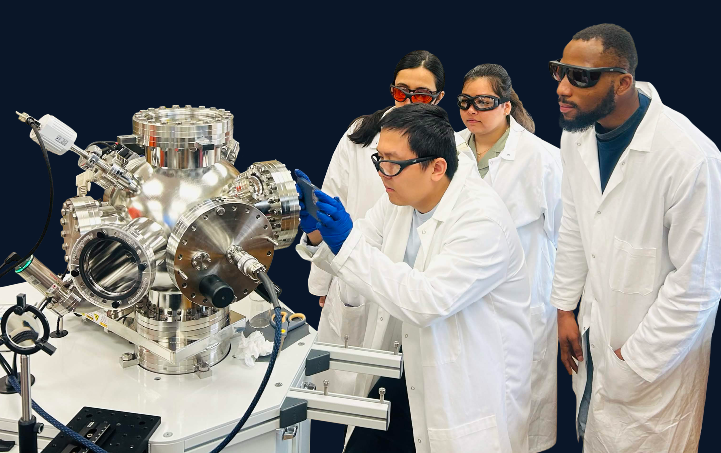
Founded by a Physicist. Trusted by Labs Worldwide.
Founded in 2000 and led by Dr. R.D. Vispute — a PhD physicist who has spent his career in materials research — Blue Wave Semiconductors builds deposition systems for research, defense, and industry. Talk directly with scientists who have real-world experience running these processes.
Our Top Products
At Blue Wave Semiconductors, we provide high-quality semiconductor fabrication equipment and advanced research technologies.
See Blue Wave Systems in Action
Explore live demonstrations and key capabilities of our custom semiconductor deposition equipment.
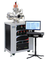
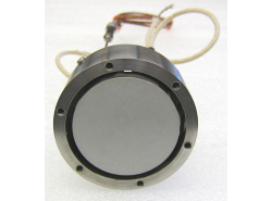
Blue Wave Semi Pulsed Laser Deposition
The PLD System offers a variety of built-in and custom features such as an optimized 6-target carousel, a substrate heater, pressure adjustment, and is designed for easy integration with a variety of other deposition techniques and sources such as: Sputtering, Thermal Evaporation & CVD, E-beam, and more.
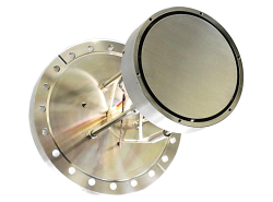
View SpecificationsSputtering Process
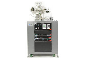
Sputtering is a process whereby atoms are ejected from a solid target material due to bombardment of the target by energetic ions. It is commonly used for thin-film deposition, etching and analytical techniques. Sputter deposition is a physical vapor deposition (PVD) method of depositing thin films by sputtering material onto a substrate.
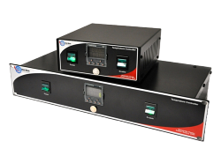
View SpecificationsHFCVD Heater Z and Rotation Stage
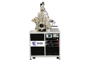
Blue Wave Substrate/Wafer rotation products are capable of reaching up 700°C while rotating up to 10-20 rpm. Compatible with reactive sputtering, PLD, PVD, e-beam and thermal evaporation, PECVD, ALD, in UHV or inert (Ar, N2, He, H2) and reactive O2, CO2, C2H2, CH4, NH3, SiH4, and metal-organic precursors, compatible to vacuum 10E-8 Torr through processing gas pressure of 1 atm.
View SpecificationsWhat Our Clients Say
Hear from researchers, engineers, and industry partners who trust Blue Wave Semiconductors to deliver advanced deposition solutions and drive innovation.
“Blue Wave Semiconductors has been an invaluable partner for our diamond coating research. The film quality and consistency exceeded our expectations.”
“The DEAR MPCVD system delivered exceptional results for our device prototyping. Their team is knowledgeable, responsive, and easy to work with.”
“From process development to large-area deposition, Blue Wave Semiconductors provides world-class capabilities and outstanding technical support.”

“We rely on Blue Wave for complex coatings that demand precision and repeatability. Their attention to detail is second to none.”

“Excellent communication, fast turnaround, and high-quality films. Blue Wave Semiconductors is our go-to partner for advanced thin film solutions.”

“The team at Blue Wave combines deep expertise with state-of-the-art equipment to deliver results that drive our innovation forward.”

How We Work With You
Start With a Conversation
Tell us what you want to achieve. You’ll speak directly with experienced scientists who know these processes inside out and know the right questions to ask.
We Plan It Together
We custom-configure your system around your process—tailoring chamber design, materials, parameters, and accessories to your exact lab requirements.
A Relationship, Not a Transaction
Our commitment doesn't end at delivery. Reach out directly anytime for process advice, spare parts, or future equipment upgrades.